- Home
- About Us
- Industry
- Services
- Reading
- Contact Us
Semiconductor Metrology and Inspection Market: Current Analysis and Forecast (2025-2033)
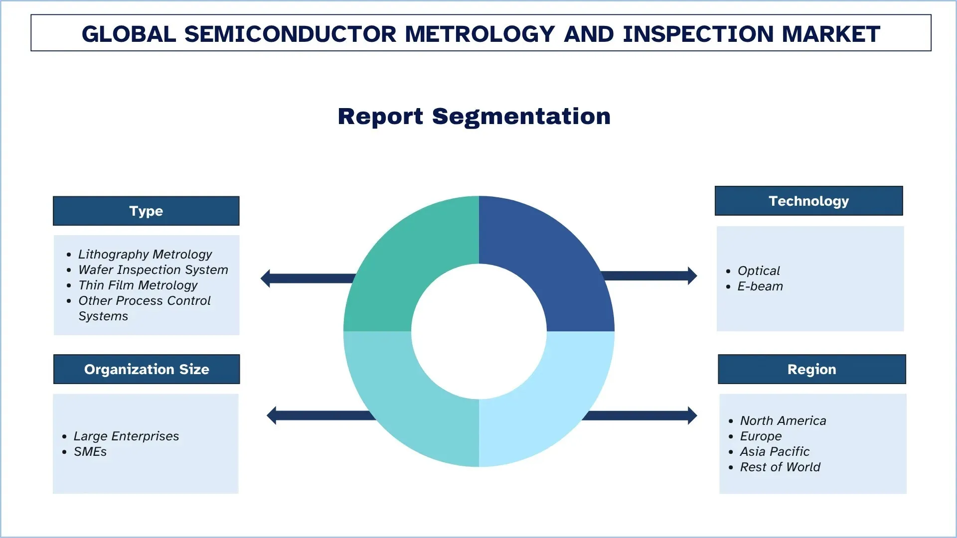
Emphasis on Type (Lithography Metrology, Wafer Inspection System, Thin Film Metrology, and Other Process Control Systems); Technology (Optical and E-beam); Organization Size (Large Enterprises and SMEs); and Region/Country
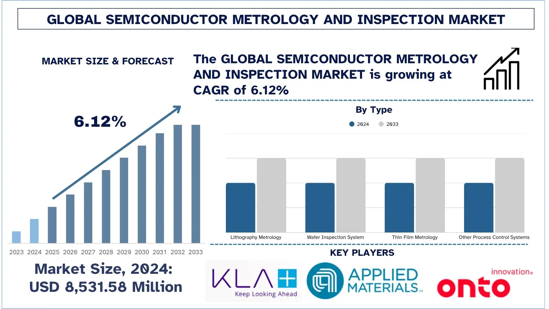
Global Semiconductor Metrology and Inspection Market Size & Forecast
The Global Semiconductor Metrology and Inspection Market was valued at USD 8,531.58 million in 2024 and is expected to grow at a CAGR of around 6.12% during the forecast period (2025–2033F), driven by the increasing demand for high-performance chips in advanced electronics, artificial intelligence, and automotive applications.
Semiconductor Metrology and Inspection Market Analysis
The existing Semiconductor Metrology and Inspection market has a high growth rate due to an ever-increasing number of requirements for smaller, more powerful, and more efficient chips in sophisticated electronics, AI, and automotive markets. With nodes at or below 5nm, it becomes increasingly important to have accuracy in the detection of defects and the accuracy of the process. The need for reliable metrology and inspection products is related to the enhancement of the yield and control of the processes that have to be performed within the semiconductor fabrication cycle, starting with the sequence of inspection actions that establish patterns over the surface of the wafer and ending with the packaging of the semiconductor devices. Advanced alternatives to plasma inspection include optical metrology, advanced X-ray inspection, and e-beam inspection, which is gaining popularity as they have a high resolution capacity. On the other hand, additional advanced inspection equipment is needed with the increase in EUV lithography progression, 3D chip structures, and heterogeneous integration.
Global Semiconductor Metrology and Inspection Market Trends
This section discusses the key market trends that are influencing the various segments of the global semiconductor metrology and inspection market, as found by our team of research experts.
AI and Machine Learning Integration
One of the central trends shaping the Semiconductor Metrology and inspection market is the use of Artificial intelligence (AI) and Machine learning (ML). The amount of process data and its complexity have been going up, too, since there is a lot of data generated with shrinking node size and complex chip architecture. Metrology tools are now integrating AI and ML technologies to work through massive amounts of data in real time, which results in predictive maintenance, pattern recognition, and automatic classification of defects. Such intelligent systems enable manufacturers to detect the anomalies in the process within the shortest period of time, optimize the inspection processes, and advance yield without any human interaction. AIs can also help tune inspection parameters on a dynamic basis using historical data, minimize false positives, and increase the accuracy of the measurements. This tendency facilitates a more rapid decision-making and a more responsive process control that is vital in high-throughput and high-precision systems such as semiconductor fabs. With fabs increasingly adopting smart manufacturing and Industry 4.0 concepts, there will be an even faster implementation of AI-enabled inspection and measurement applications as the key factor in efficient and cost-effective semiconductor manufacturing.
Semiconductor Metrology and Inspection Industry Segmentation
This section provides an analysis of the key trends in each segment of the global semiconductor metrology and inspection market report, along with forecasts at the global, regional, and country levels for 2025-2033.
The Wafer Inspection System Dominates the Semiconductor Metrology and Inspection Market
Based on type, the Semiconductor Metrology and Inspection market is segmented into Lithography Metrology, Wafer Inspection Systems, Thin Film Metrology, and Other Process Control Systems. In 2024, the Wafer Inspection System segment dominated the market and is anticipated to continue its leadership throughout the forecast period. With the move of semiconductor nodes to 5nm or less, process validation and accuracy in identifying the defects are critical to process optimization. Wafer inspection systems, through technologies such as e-beam and optical inspection, can perform surface and sub-surface defect inspection in high resolutions over front-end and back-end processes. These systems enable quick detection of the anomalies, thus providing higher reliability of the chips and reducing losses in production. Advanced heterogeneous integration in advanced packaging and the increasing complexity of 3D structures have also driven the demand. Such systems guarantee adherence to strict performance requirements in high-value applications, such as AI processors, automotive silicon, and memory. Driven by the escalating production required by the chip-making industry, the inspection technology serving the wafer industry is emerging as a pivot supporting the key quality, scale, and sustained competitiveness of the chip supply chain globally.
Optical Technology held the Largest Market Share in the Semiconductor Metrology and Inspection Market.
Based on technology, the Semiconductor Metrology and Inspection market is segmented into Optical and E-beam systems. In 2024, the Optical segment dominated the market and is expected to maintain its lead throughout the forecast period. The popularity of optical inspection systems is attributed to low cost, high throughput, and the non-destructive nature of the system to detect surface defects and critical dimensions variances over wafers. These systems are very important in the front and back of semiconductor manufacturing, particularly in high-volume production of logic and memory devices. These systems are important in front-end and back-end production of semiconductors such as logic devices and memory at the wafer-level production. Their use in high-level lithography nodes, 3D NAND, and FinFET technologies has now become crucial in terms of quality assurance. Due to the increasingly complex shapes of chips and increasingly narrow process tolerances, optical metrology is continually evolving to provide real-time, precise measurements relevant to yield improvement and achieve the scale of manufacturing in semiconductor fab facilities.
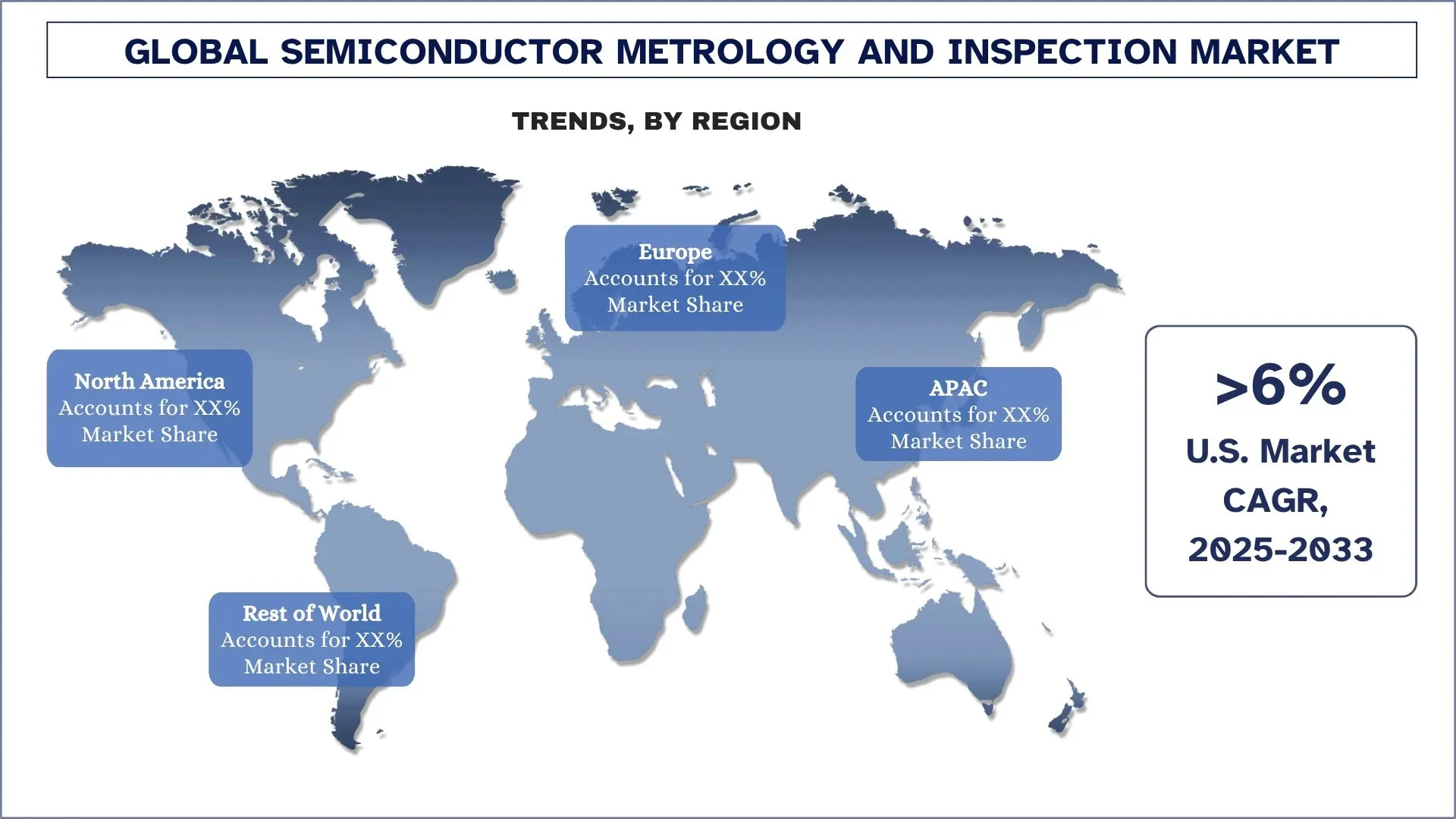
North America Dominated the Global Semiconductor Metrology and Inspection Market
North America is now the top-ranked region in Semiconductor Metrology and Inspection and is likely to remain in the top position in the future as well. This leadership has been brought about by a dominance of high-end semiconductor foundries, technology-intensive fab facilities, and a healthy ecosystem of equipment suppliers. The buoyancy of investments in R&D helps the region thrive since recent federal investment in the CHIPS and Science Act has increased domestic semiconductor manufacturing and innovation. The leaders of the US industry are working on state-of-the-art metrology and inspection technologies that can qualify the next generations of module sizes, such as EUV cell and 3D chip designs. The advances in high-performance computing, AI chips, and electric vehicles are driving the industry to higher-performance inspection systems. Furthermore, the presence of leading research and technological companies and organizations ensures a constant stream of innovation and talent. Another future theme is overall chip complexity, which is continuing to increase, and North America specializes in reliability, defect-reduction, and quality-control, thus maintaining its leadership in the market.
U.S. held a dominant Share of the North America Semiconductor Metrology and Inspection Market in 2024
The U.S. is becoming a global hub for the semiconductor metrology and inspection industry due to the must-see federal programs like the CHIPS and Science Act, the Inflation Reduction Act, and increased R&D dollar allocations to the National Semiconductor Technology Center (NSTC). Significant investments are pouring into advanced fabrication plants in the states such as Arizona, Texas, and New York, with the help of public grants as well as personal finances. The presence of innovation clusters between Silicon Valley, Boston, and Austin is fast-tracking the process of innovation, as precision metrology tool development is based on advancements in AI, optical, and e-beam inspection systems. The Department of Commerce and the Department of Energy are directing funds towards the domestic expansion of capabilities throughout the chip supply chain, including the materials, packaging, and course control equipment. Top-tier talent is offered by universities, national labs, and partners to perform research in the next-gen inspection. The advantages make the U.S one of the most rapidly expanding markets, as well as a strategic headquarters location of semiconductor metrology innovation in the entire world.
Semiconductor Metrology and Inspection Industry Competitive Landscape
The global semiconductor metrology and inspection market is competitive, with several global and international market players. The key players are adopting different growth strategies to enhance their market presence, such as partnerships, agreements, collaborations, new product launches, geographical expansions, and mergers and acquisitions.
Top Semiconductor Metrology and Inspection Companies
Some of the major players in the market are KLA Corporation, Applied Materials, Inc., Onto Innovation, Thermo Fisher Scientific Inc., Hitachi, Ltd., Nova Ltd., Lasertec Corporation, JEOL Ltd., Camtek, and Nikon Metrology Inc.
Recent Developments in the Semiconductor Metrology and Inspection Market
In January 2025, Koh Young joined forces with NTV USA to grow its existing semiconductor metrology and inspection solutions in the United States. The partnership introduces Meister Series systems and ZenStar systems, adding to the SiP, WLP, and die stacking package inspection. Koh Young has the potential to enhance yield, quality, and quality defect, using deep learning and 3D measurement technology in the future of advanced semiconductor packaging.
In July 2023, Applied Materials and Fraunhofer IPMS opened an over 2000 m 2 large semiconductor metrology center at Silicon Saxony in Dresden. The hub has eBeam metrology systems, including the VeritySEM CD-SEM, that boost the inspection of wafers, process control, and R&D on the ICAPS markets. This partnership supercharges the European processes of learning, metrology, and semiconductor manufacturing precision.
Global Semiconductor Metrology and Inspection Market Report Coverage
Report Attribute | Details |
Base year | 2024 |
Forecast period | 2025-2033 |
Growth momentum | Accelerate at a CAGR of 6.12% |
Market size 2024 | USD 8,531.58 Million |
Regional analysis | North America, Europe, APAC, Rest of the World |
Major contributing region | North America is expected to dominate the market during the forecast period. |
Key countries covered | U.S., Canada, Germany, U.K., Spain, Italy, France, China, Japan, South Korea, and India |
Companies profiled | KLA Corporation, Applied Materials, Inc., Onto Innovation, Thermo Fisher Scientific Inc., Hitachi, Ltd., Nova Ltd., Lasertec Corporation, JEOL Ltd., Camtek, and Nikon Metrology Inc. |
Report Scope | Market Trends, Drivers, and Restraints; Revenue Estimation and Forecast; Segmentation Analysis; Demand and Supply Side Analysis; Competitive Landscape; Company Profiling |
Segments Covered | By Type; By Technology; By Organization Size; By Region/Country |
Reasons to Buy Semiconductor Metrology and Inspection Market Report:
The study includes market sizing and forecasting analysis confirmed by authenticated key industry experts.
The report briefly reviews overall industry performance at a glance.
The report covers an in-depth analysis of prominent industry peers, primarily focusing on key business financials, type portfolios, expansion strategies, and recent developments.
Detailed examination of drivers, restraints, key trends, and opportunities prevailing in the industry.
The study comprehensively covers the market across different segments.
Deep dive regional-level analysis of the industry.
Customization Options:
The global semiconductor metrology and inspection market can further be customized as per the requirements or any other market segment. Besides this, UnivDatos understands that you may have your own business needs; hence, feel free to contact us to get a report that completely suits your requirements.
Table of Content
Research Methodology for the Global Semiconductor Metrology and Inspection Market Analysis (2023-2033)
We analyzed the historical market, estimated the current market, and forecasted the future market of the global semiconductor metrology and inspection market to assess its application in major regions worldwide. We conducted exhaustive secondary research to gather historical market data and estimate the current market size. To validate these insights, we carefully reviewed numerous findings and assumptions. Additionally, we conducted in-depth primary interviews with industry experts across the semiconductor metrology and inspection value chain. After validating market figures through these interviews, we used both top-down and bottom-up approaches to forecast the overall market size. We then employed market breakdown and data triangulation methods to estimate and analyze the market size of industry segments and sub-segments.
Market Engineering
We employed the data triangulation technique to finalize the overall market estimation and derive precise statistical numbers for each segment and sub-segment of the global semiconductor metrology and inspection market. We split the data into several segments and sub-segments by analyzing various parameters and trends, including type, technology, organization size, and regions within the global semiconductor metrology and inspection market.
The Main Objective of the Global Semiconductor Metrology and Inspection Market Study
The study identifies current and future trends in the global semiconductor metrology and inspection market, providing strategic insights for investors. It highlights regional market attractiveness, enabling industry participants to tap into untapped markets and gain a first-mover advantage. Other quantitative goals of the studies include:
Market Size Analysis: Assess the current market size and forecast the market size of the global semiconductor metrology and inspection market and its segments in terms of value (USD).
Semiconductor Metrology and Inspection Market Segmentation: Segments in the study include areas of type, technology, organization size, and regions.
Regulatory Framework & Value Chain Analysis: Examine the regulatory framework, value chain, customer behavior, and competitive landscape of the semiconductor metrology and inspection industry.
Regional Analysis: Conduct a detailed regional analysis for key areas such as Asia Pacific, Europe, North America, and the Rest of the World.
Company Profiles & Growth Strategies: Company profiles of the semiconductor metrology and inspection market and the growth strategies adopted by the market players to sustain the fast-growing market.
Frequently Asked Questions FAQs
Q1: What is the global semiconductor metrology and inspection current market size and its growth potential?
The global semiconductor metrology and inspection market was valued at USD 8,531.58 million in 2024 and is expected to grow at a CAGR of 6.12% during the forecast period (2025-2033).
Q2: Which segment has the largest share of the global semiconductor metrology and inspection market by type?
The Wafer Inspection System segment dominated the market and is expected to maintain its leadership throughout the forecast period, driven by the rising demand for defect detection and process control in advanced semiconductor manufacturing.
Q3: What are the driving factors for the growth of the global semiconductor metrology and inspection market?
• Shrinking Node Sizes: As chips move to sub-5nm and 3nm geometries, precise metrology and defect detection become critical for yield and performance.
• Growth of Advanced Packaging & 3D ICs: Complex chip structures require accurate inspection across multiple layers, driving demand for high-resolution metrology tools.
• Increased Demand from AI, HPC, and Automotive Sectors: These high-performance applications require strict process control and quality assurance throughout the semiconductor value chain.
Q4: What are the emerging technologies and trends in the global semiconductor metrology and inspection market?
• AI and Machine Learning Integration: AI-powered analytics are being used for predictive maintenance, defect classification, and process optimization in real time.
• Adoption of E-beam and Hybrid Metrology Tools: Electron beam-based and hybrid inspection systems are gaining popularity for their high-resolution capabilities.
• Shift to In-Line and Real-Time Metrology: Demand is growing for inspection solutions that offer real-time insights during production to reduce yield loss.
Q5: What are the key challenges in the global semiconductor metrology and inspection market?
• High Capital Investment: Advanced metrology systems are expensive to develop and deploy, limiting accessibility for smaller fabs or new entrants.
• Complexity in 3D Structures and Materials: Accurate inspection of multi-layered and heterogeneous materials is increasingly complex, especially with emerging architectures.
• Data Overload and Integration Issues: Metrology tools generate large volumes of data, requiring advanced analytics and seamless integration with fab workflows.
Q6: Which region dominates the global semiconductor metrology and inspection market?
North America currently leads the semiconductor metrology and inspection market and is expected to maintain its dominance during the forecast period. This leadership is primarily driven by the presence of major semiconductor foundries, advanced R&D infrastructure, and robust federal initiatives supporting domestic chip manufacturing and process innovation.
Q7: Who are the key players in the global semiconductor metrology and inspection market?
Some of the key companies include:
• KLA Corporation
• Applied Materials, Inc.
• Onto Innovation
• Thermo Fisher Scientific Inc.
• Hitachi, Ltd.
• Nova Ltd.
• Lasertec Corporation
• JEOL Ltd.
• Camtek
• Nikon Metrology Inc.
Q8: What intellectual-property strategies are companies using to secure and monetize semiconductor metrology and inspection innovations?
• Process-Specific Patents: Firms are securing IP on critical process innovations such as hybrid metrology platforms, e-beam inspection algorithms, and AI-driven defect classification engines.
• Licensing Frameworks: Leading OEMs license proprietary technologies (e.g., advanced optics, sensor arrays) to toolmakers and fabs, enabling revenue streams while controlling IP usage.
• Strategic Trade Secrets: Companies retain core software code, calibration techniques, and image-processing heuristics as trade secrets to maintain a competitive edge while minimizing exposure.
Q9: How are supply-chain partnerships evolving to secure critical components for semiconductor metrology and inspection tools?
Component Co-Development: Toolmakers are collaborating with optics, sensors, and stage system providers to co-engineer modules tailored for next-gen nodes and 3D chip structures.
• Secure Supplier Alliances: Long-term agreements with specialized manufacturers ensure a stable supply of precision lenses, electron beam sources, and vacuum subsystems.
• Localization Strategies: To mitigate geopolitical risk and reduce lead times, companies are regionalizing key assembly operations and sourcing partners near major fab clusters in Asia, North America, and Europe.
Related Reports
Customers who bought this item also bought


Ion Beam Etching System Market: Current Analysis and Forecast (2026-2034)
Emphasis on Type (Conventional Ion Beam Etching (IBE), Reactive Ion Beam Etching (RIBE), Focused Ion Beam (FIB) Systems, Automatic Ion Beam, and Others); Application (Semiconductor Manufacturing, Microelectronics & Data Storage, Photonics & Optoelectronics, MEMS (Micro-Electro-Mechanical Systems), Research & Metrology, and Others); End User (Semiconductor & Electronics, Aerospace & Defense, Healthcare & Medical Devices, Research Institutions, and Others); and Region/Country
April 30, 2026


Power over Ethernet (PoE) Chipset Market: Current Analysis and Forecast (2025-2033)
Emphasis on Type (PoE Power Sourcing Equipment (PSE) Chipset and PoE Powered Devices (PD) Chipset); Standard (IEEE 802.3at Standard, IEEE 802.3bt Standard, and IEEE 802.3af Standard); Device (IP/Network Cameras, VoIP Phone, Ethernet Switch & Injector, Wireless Radio Access Point, Proximity Sensor, LED Lighting, and Others); End-use (Commercial, Industrial, and Residential); and Region/Country
April 17, 2026